Search the Community
Showing results for tags 'mosfet'.
-

False Turn-On in MOSFET Driving Circuit and Countermeasures
vbsemi posted a topic in Theory articles
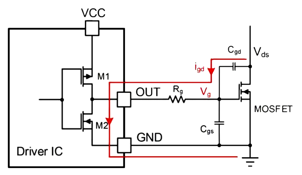
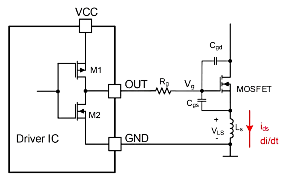
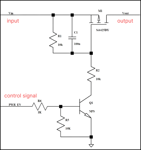
https://www.youtube.com/watch?v=PwOTTqUo9tA MOSFET is a switch controlled by gate voltage. When the gate voltage is greater than the turn-on threshold, the MOSFET is turned on; when the gate voltage is lower than the turn-on threshold, the MOSFET is turned off. In actual applications, due to the influence of other factors such as device and peripheral circuit parasitic parameters, the originally turned-off power device may be mistakenly turned on. Today, let's talk about the mistaken turn-on of MOSFET in the drive circuit and its countermeasures. Let's talk about two cases of mistaken turn-on: mistaken turn-on caused by Miller effect and mistaken turn-on caused by parasitic inductance. False turn-on caused by Miller effect When the MOSFET is turned off and then turned on, the Vds voltage (the maximum voltage that can be applied between the drain and the source) rises rapidly to produce a high dv/dt (the rate of change of the drain-source voltage during the switching transient), thereby generating a displacement current (igd) in the capacitor Cgd (Miller capacitor). This displacement current will generate a voltage spike after flowing through . If this voltage spike exceeds the turn-on threshold of the MOSFET, the MOSFET will be turned on, causing the circuit to be turned on or even damaged. Another type of false turn-on is caused by parasitic inductance on the line. As shown in the figure below, Ls is the parasitic inductance on the source of the MOSFET. When the MOSFET is turned off quickly, the current decreases rapidly to produce a high di/dt, and then a negative voltage (VLS) is generated across the two ends of the parasitic inductance. If this VLS voltage exceeds the gate threshold of the MOSFET, the MOSFET will be turned on by mistake. So, what methods do we have to deal with the phenomenon of MOSFET being turned on by mistake? 1. Adjust the gate drive resistor and capacitor The turn-on/off speed of the MOSFET can be adjusted by adjusting the size of the gate drive resistor and capacitor: increase the gate drive resistor and capacitor to slow down the turn-on/off speed of the MOSFET, reduce dv/dt (di/dt) and thus reduce the gate voltage spike. 2. Add a transistor A transistor can be placed near the gate of the power tube to prevent false opening during the shutdown period, effectively suppressing the false gate opening caused by the Miller effect. 3. Use an anti-parallel diode The current in the inductor can disappear through the diode loop, thereby avoiding the generation of reverse potential.-
- mosfet
- semiconductor
-
(and 2 more)
Tagged with:
-
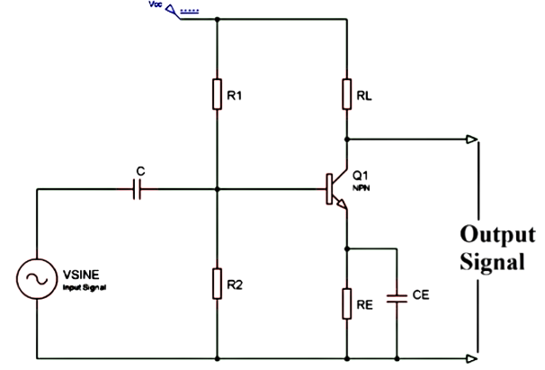
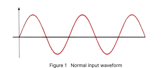
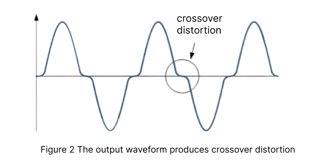
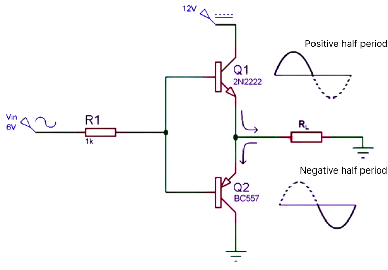
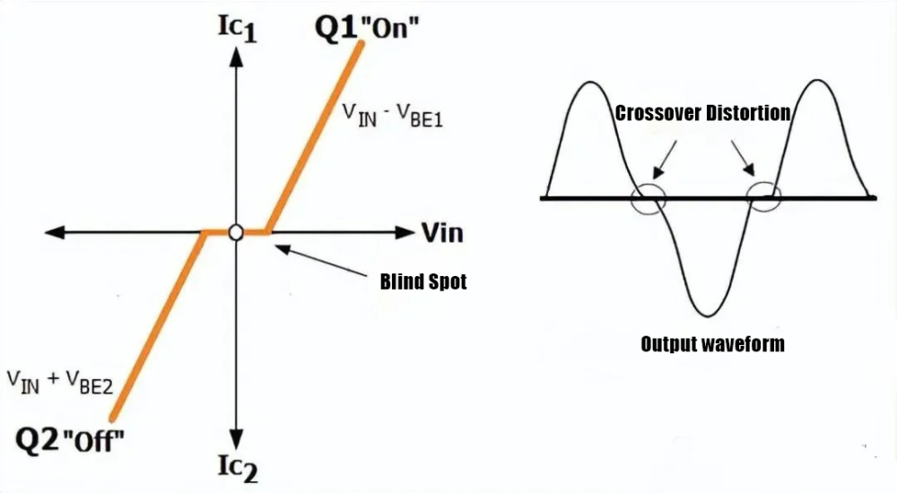
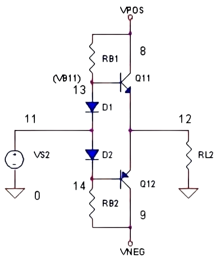
We know that push-pull circuits come in many types, such as class A or class B amplifiers. Class B amplifiers are the ones used in practical applications. They are more efficient than class A, but they are often affected by crossover distortion. So how does it affect it? How can it be reduced? When the signal is distorted at 0V, the transistor will provide a voltage of 0.7v at the base-emitter junction before turning on. When the AC input voltage is applied to the push-pull amplifier, it increases from 0 until it reaches 0.7V, and the transistor remains off without any output. So why does crossover distortion occur when VIN reaches zero? (Class B amplifier) In fact, transistors Q1 and Q2 cannot be turned on at the same time. If Q1 is turned on, VIN must be greater than Vout, and if Q2 is turned on, Vin must be less than Vout. If VIN is equal to zero, Vout must also be equal to zero. When VIN increases from zero, the output voltage Vout will also remain at zero. Until V IN is less than 0.7V, the output voltage shows a dead zone, and the same situation will occur when V IN starts to decrease from zero. How to reduce the crossover distortion of the push-pull transistor circuit? It can be corrected by using two diodes that are turned on at the transistor position, that is, the class AB amplifier circuit. It uses the characteristics of both. From 0V to 0.7V, the diode is biased in the on state to make up for the 0.7 V loss of the emitter follower. At this time, the transistor has no signal at the base, which solves the crossover distortion problem. In addition, it can also be achieved by reducing the resistance value. This is because the resistor RB1 controls the current of D1. The smaller RB1 is, the greater the current is, that is, the greater the voltage of the diode is, so when there is no input signal, the Vbe will be greater. This increased deviation will further reduce the distortion. However, the specific application situation is still based on the actual circuit design.
-
- mosfet
- semiconductor
- (and 4 more)
-
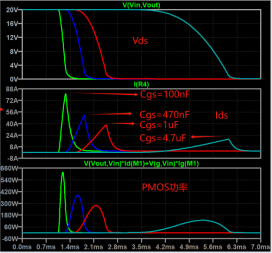
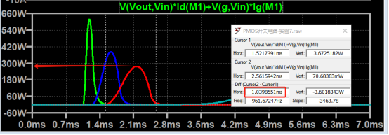
提到MOS管烧毁,一般是因为它非工作在SOA工作区,还有一种情况就是MOS管过流了。 比如这个电路中PMOS管最大允许的电流是50A,在MOS管开启瞬间最大电流达到了80+,那这个电流就非常大了。 此时的PMOS属于超规格使用了,我们可以在SOA曲线上看出,它并没有工作在SOA区间,这将会导致PMOS损坏。 那如果选择更高电流的PMOS呢?当然可以,但是成本会更高。 我们可以选择调节下外围电阻或者电容,让PMOS开通的速度更慢,这样电流就可以降下来。 比如调整R1,R2,还有gs之间的跨接电容,当Cgs调整为1uF时,Ids最大只有40A,在电流方面这就可以了,并且满足了80%的降额。 (50安培*0.8=40安培) 接下来我们看功率方面,从SOA曲线上看,MOS管的开通时间约为1ms,此时的最大功率是280W。 芯片正常热阻是50°C/W,最高结温可以是302°F。 假设环境温度是77°F,那么1ms能承受的瞬间功率大概在357W。 这里的 PMOS实际功率在280W,并没有超过限制,也就是说它正常工作在SOA区。 因此,当MOS管开通瞬间电流冲击较大时,可以适当调整Cgs电容,让PMOS 工作在SOA区,就可以避免MOS损坏的问题了。
-
- mosfet
- overcurrent,
-
(and 1 more)
Tagged with:
-
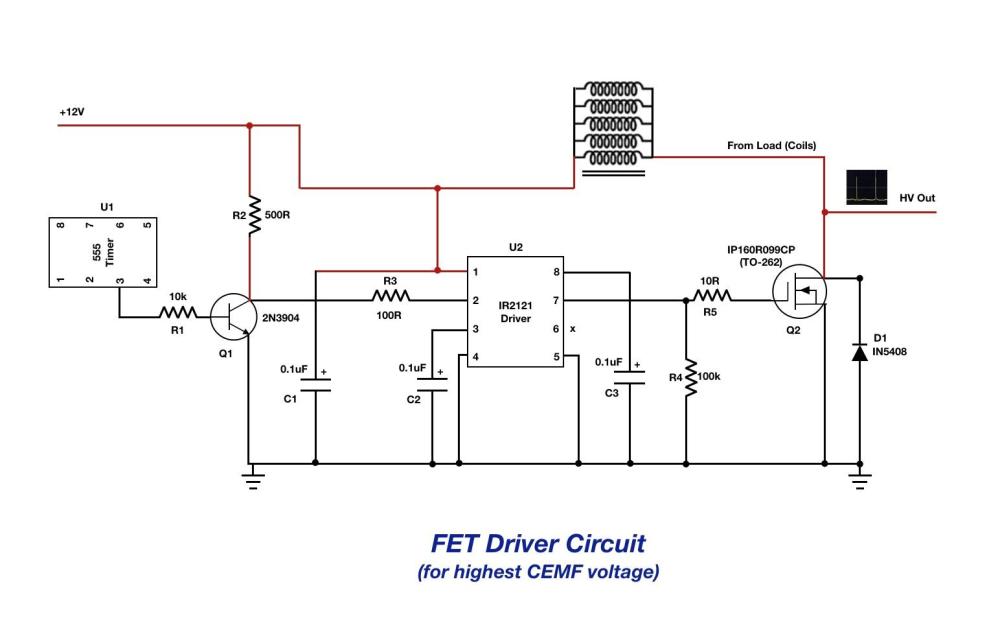
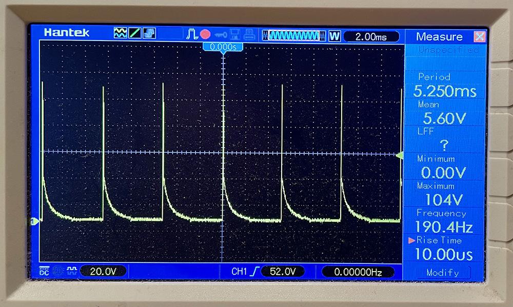
I have built a circuit for which the aim is to produce high voltage back EMF spikes from the Drain of a MOSFET so I can investigate some of the properties of these voltage transients. What I have built is shown in the attached circuit where I am using an IR2121 driver chip to encourage shorter shut off times and so produce higher voltage spikes. Going from a circuit that didn't use a driver chip to one that does has increased the voltage from about 800V to 1,040V as shown in the scope image using a 10:1 voltage divider. I have read that there are ways to further reduce the FET shut off time but as electronics is not my main discipline I find them rather confusing. For example, reducing the Gate bias resistor (R5) further (to 5R?) or putting a small capacitor (1nF?) across R5 and keeping the PCB track resistance from R5 to the Gate of Q2 as short as possible. I would appreciate any suggestions. Thanks
-
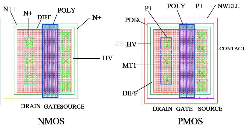
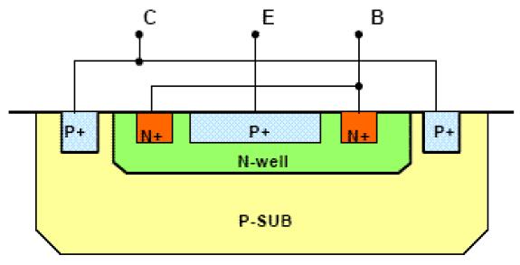
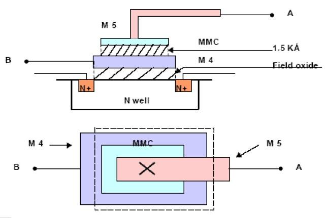
PCB Layout Tutorial: For High-Quality PCB Design http://www.apogeeweb.net/article/89.html Asymmetric source/drain MOS transistor LPNP MMC
-
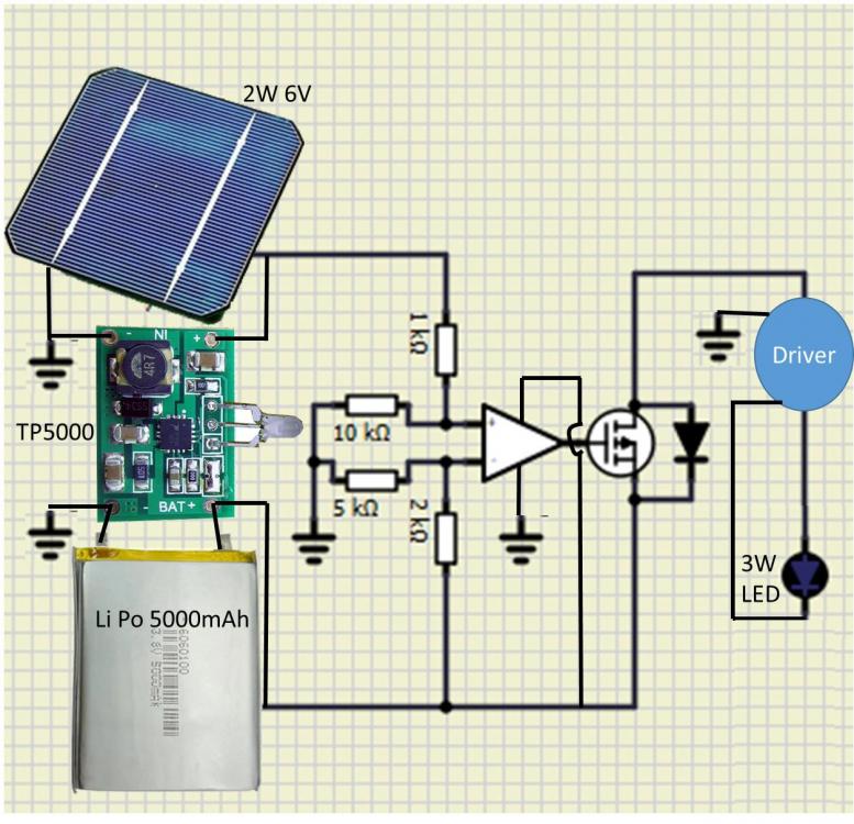
Hello. I would like to make a garden solar lamp that automatically turn on when the sun goes down. I tryed first with a transistor s9013 npn (seen on youtube), but it restricted the current, i suspect because of the internal resistance of the transistor. I decided to try the use of an Op amp as comparator, with a low internal resistance P channel Mosfet. I don't have much experience with these components, and the best way of learning is trying right? So see below my circuit. My problem is that it seem to work fine when the battery is full but the solar charging doesn't seem to be very efficient (the charge light does turn ON) and the battery looses it's charge fast, leading to a weired blinking LED. would anyone see a problem with my circuit explaining that? thank you very much for your help Best Damien

